
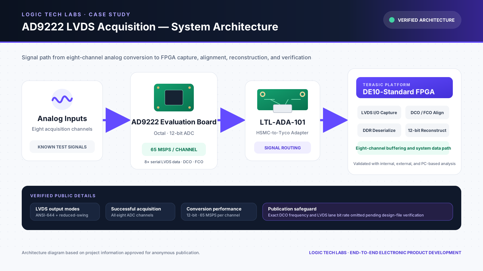
Interfacing a serial-output ADC board to an FPGA is not only a connector-mapping exercise. The receiver must preserve the electrical interface, capture source-synchronous data at the correct phase, reconstruct sample words, establish channel alignment, and move the data safely into the rest of the system.
The AD9222 integrates eight 12-bit ADC channels and provides serial LVDS data together with a data clock output (DCO) and frame clock output (FCO). The device datasheet identifies ANSI-644 serial LVDS as the default output mode. This article focuses on the engineering structure of a reliable receiver rather than on a vendor-specific HDL implementation.
Key engineering takeaways
- ✓Treat the ADC, adapter, FPGA pins, I/O standard, termination, and timing constraints as one interface.
- ✓Capture the serial data in the DCO domain before moving reconstructed words into a system clock domain.
- ✓Use the ADC's repeatable digital test pattern before relying on an analog input.
- ✓Verify one channel and one clock relationship first, then scale to all eight channels.
- ✓Preserve raw capture evidence and configuration data so a successful bench result is reproducible.
1. Start from the converter's actual output model
Each AD9222 channel produces a serial differential data stream. DCO is the source-synchronous clock used to capture the serialized bits, while FCO marks the sample-word boundary. These three signal roles must remain distinct in the architecture: DCO is a capture clock, FCO is framing information, and each data pair carries one channel's serialized sample stream.
At the maximum 65 MSPS operating point, a 12-bit sample must be serialized within each sample interval. The exact DCO relationship, bit order, output mode, and alignment settings must be taken from the selected device configuration and datasheet rather than inferred from the connector alone.
| Signal group | Receiver role | Primary design concern |
|---|---|---|
| Eight serial data pairs | Carry channel sample bits | Polarity, pin mapping, skew, and bit order |
| DCO pair | Source-synchronous capture clock | Input clocking resource, phase, and timing margin |
| FCO pair | Marks the sample frame | Word boundary and deterministic alignment |
| SPI/control | Configures output and test modes | Known register state and repeatable startup |
2. Define the physical and electrical interface before writing RTL
Create a controlled pin-mapping document from the ADC evaluation-board connector to the adapter and then to the FPGA package pins. Record the positive and negative sides of every pair, the FPGA I/O bank, the bank voltage, the selected I/O standard, and any termination implemented on the board or inside the FPGA.
An adapter can preserve connectivity while still degrading timing margin if it introduces long stubs, inconsistent reference planes, or poorly controlled differential geometry. The PCB stack-up and connector transition therefore belong in the same review as the HDL receiver.
- Confirm that every differential pair reaches a suitable differential-capable FPGA input.
- Check FPGA-bank voltage and I/O-standard compatibility before assembly or power-up.
- Document where the differential termination is located and avoid accidental double termination.
- Constrain the PCB geometry from the actual fabricator stack-up, not only from a generic trace-width rule.
- Keep a polarity record; do not rely on later HDL inversion to conceal an undocumented mapping error.
3. Partition the FPGA receiver into testable stages
A maintainable receiver separates input capture from sample assembly and separates sample assembly from transport. This makes it possible to inspect the boundary at which an error first appears instead of debugging a monolithic acquisition block.
The usual structure is: differential input buffer, DCO-domain DDR capture, per-channel shift or deserializer logic, FCO-based word alignment, channel-valid generation, and a clock-domain crossing buffer into the processing or host-transfer clock domain.
- 01
Input and clock resources
Use device-appropriate differential input buffers and route DCO through the clock network recommended for the selected FPGA family.
- 02
DDR capture
Sample incoming bits on both DCO edges using dedicated input or DDR resources where available.
- 03
Word reconstruction
Assemble the captured bit sequence into 12-bit samples with an explicit, documented bit order.
- 04
Frame alignment
Use FCO to establish the sample boundary and detect loss of alignment rather than assuming power-up phase.
- 05
Clock-domain crossing
Transfer complete samples through a defined CDC structure such as an asynchronous FIFO or a reviewed handshake.
- 06
Instrumentation
Expose alignment state, error counters, test-pattern comparison, and capture points for laboratory debug.
4. Constrain what is physically happening
Static timing analysis is meaningful only when the generated clocks, input delays, clock relationships, and false or asynchronous paths describe the real interface. A design that compiles without correct constraints has not demonstrated capture margin.
Document the timing assumptions used to derive the constraints: ADC clocking mode, output timing, board delay, DCO relationship, FPGA input resource, and any phase adjustment. Re-run timing analysis when the adapter, FPGA family, clock setting, or ADC output mode changes.
5. Bring the interface up in a controlled sequence
The AD9222 supports built-in and custom digital test patterns. Its repeatable test pattern keeps FCO and DCO operating, which makes it useful for alignment and mapping checks before analog behavior is introduced.
A disciplined sequence reduces the number of unknowns present at each step and produces evidence that can be compared after a hardware or HDL revision.
- 01
Static inspection
Verify rails, bank voltages, connector orientation, pair mapping, continuity, and absence of shorts.
- 02
Clock observation
Confirm the ADC sample clock, DCO, and FCO at accessible points or through trusted FPGA instrumentation.
- 03
Digital test pattern
Capture the known repeating pattern on one channel and verify polarity, bit order, and word boundary.
- 04
All-channel expansion
Enable all eight channels and compare reconstructed words while monitoring alignment and error counters.
- 05
Known analog input
Apply a controlled signal and correlate FPGA samples with the expected waveform and converter configuration.
- 06
Long-duration validation
Run sustained acquisition and exercise resets, startup sequences, triggered modes, and host transport.
6. A verified LTL implementation
Logic Tech Labs implemented this architecture on a Terasic DE10-Standard platform using the LTL-ADA-101 HSMC-to-Tyco adapter. The verified system acquired all eight 12-bit AD9222 channels at 65 MSPS per channel and transferred captured data through the board's embedded-Linux path to a host over Ethernet.
That result is specific to the documented project configuration. It should not be interpreted as a universal performance guarantee for every FPGA, adapter revision, cable, clock source, or ADC configuration.
Primary references
Sources and further reading
- Analog Devices — AD9222 data sheet ↗
- Analog Devices — HSC-ADC-FPGA deserialization board data sheet ↗
- Terasic — DE10-Standard resources and user manual ↗
External documents remain the authority for component ratings, standard requirements, and device-specific implementation details.