
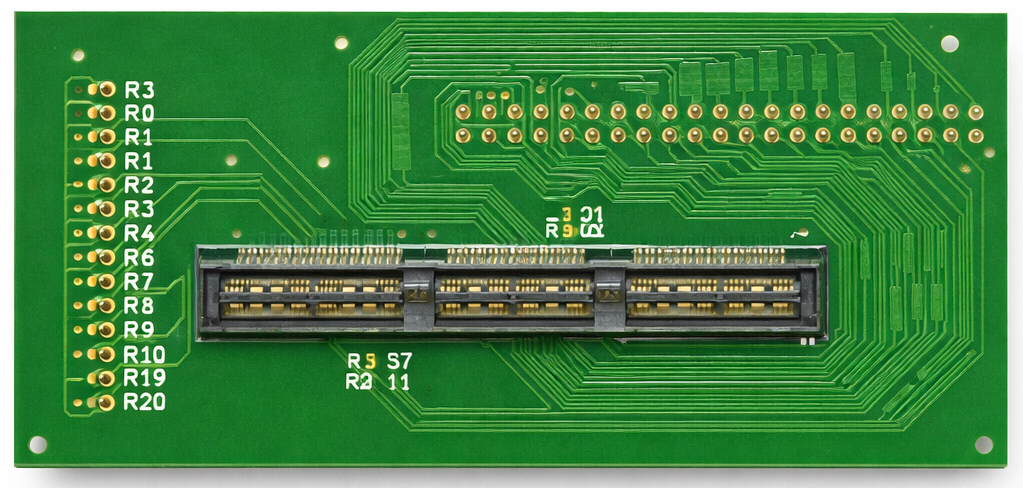
Connector names are not interchangeable descriptions of capability. HSMC, FMC, and general-purpose GPIO headers differ in standardization, available signal classes, mechanical definition, clocking resources, power expectations, and portability between FPGA platforms.
The correct adapter is the one that satisfies the complete interface contract: electrical compatibility, bandwidth, timing, pin count, clock distribution, power, mechanics, availability, and the amount of platform-specific engineering the project can accept.
Key engineering takeaways
- ✓Choose from system requirements, not from connector familiarity.
- ✓FMC is defined by ANSI/VITA 57.1; HSMC and GPIO implementations must be checked against the exact carrier-board documentation.
- ✓GPIO is flexible but the header name alone does not guarantee a signaling standard or high-speed performance.
- ✓An adapter cannot correct incompatible voltage levels, missing transceivers, inadequate clocks, or unsuitable FPGA pins without additional circuitry.
- ✓Freeze the pin map and electrical assumptions as a reviewed interface-control document.
1. What each interface is intended to provide
FMC, short for FPGA Mezzanine Card, is an industry mezzanine format defined by ANSI/VITA 57.1. VITA describes it as a compact physical interface between an I/O mezzanine and an FPGA carrier. This standardization helps portability, but an FMC carrier and mezzanine still need compatible pin assignments, voltage choices, clock resources, and supported signal classes.
HSMC is used on Intel/Altera-oriented development platforms such as the Terasic DE10-Standard. It offers a dense expansion path to FPGA I/O and is useful when both sides of the design are tied to a documented HSMC carrier. GPIO headers are simpler and broadly understandable, but their electrical and timing capability depends heavily on the individual board.
| Interface | Strong fit | Primary caution |
|---|---|---|
| HSMC | Dense FPGA expansion on a known HSMC carrier | Board-specific pinout, voltage, and platform dependence |
| FMC | Standardized mezzanine ecosystem and reusable I/O modules | LPC/HPC variant, VADJ, clocks, and carrier compatibility must match |
| GPIO | Control, moderate-speed parallel I/O, prototypes, and simple peripherals | No universal electrical or high-speed guarantee from the connector name |
2. Ask these questions before selecting the adapter
A useful selection review starts with the signals and only then maps them to a connector. Count single-ended signals, differential pairs, clocks, control lines, ground returns, and power rails. Identify directionality, voltage standards, termination, and whether any pair must use a dedicated transceiver or clock-capable pin.
- What are the maximum edge rate, toggle rate, and required timing margin?
- Which signals are single-ended, differential, source-synchronous, or asynchronous?
- Does the carrier expose the required FPGA pin type and I/O-bank voltage?
- Are dedicated reference clocks or multi-gigabit transceivers required?
- What power can the carrier safely provide, and what sequencing is required?
- What connector height, keep-out, mounting, and enclosure constraints apply?
- Must the adapter work on one named development board or across several platforms?
3. Understand what a passive adapter can and cannot do
A passive adapter can remap pins, preserve differential pairs, provide selected termination or protection components, and translate mechanical placement. It cannot make an FPGA bank tolerate an unsupported voltage, create a missing clock resource, or convert between unrelated electrical standards without active circuitry.
If voltage translation, buffering, level shifting, fan-out, protocol conversion, isolation, or power sequencing is required, the design is no longer only a pin adapter. Those functions must be treated as active hardware with their own power, timing, thermal, and verification requirements.
4. Match routing discipline to the signal, not the connector label
High-speed single-ended and differential nets need a stack-up-based routing plan. The relevant impedance is set by the driver, receiver, topology, and interconnect—not by whether the connector is called HSMC, FMC, or GPIO.
For LVDS, Texas Instruments' layout guidance calls for 100-ohm differential routing, close coupling, intra-pair length symmetry, short direct routes, minimized stubs, and termination close to the receiver. The actual geometry must be calculated with the selected laminate and fabricator stack-up.
5. Use a documented selection workflow
A repeatable process makes the interface decision reviewable and reduces late changes after schematic capture or layout has begun.
- 01
Capture the signal inventory
List every signal, pair, clock, rail, ground requirement, direction, and electrical standard.
- 02
Audit the carrier
Check the exact board manual, connector table, FPGA package pins, I/O banks, clocks, and power limits.
- 03
Score candidate interfaces
Compare pin capacity, electrical fit, bandwidth, mechanics, portability, procurement, and development risk.
- 04
Define the adapter architecture
Separate passive mapping from any required active translation, buffering, protection, or power functions.
- 05
Review the pin map
Freeze a controlled interface document before layout and verify it against both endpoint schematics.
- 06
Plan bring-up
Include loopback, test patterns, clock observation, safe power-up, and accessible measurement points.
6. Logic Tech Labs adapter paths
The LTL catalog includes HSMC-to-Tyco, HSMC-to-GPIO, GPIO-to-FMC, and GPIO-to-parallel-edge adapters. Each product page separates supplied information from fields that still require project-specific confirmation.
When no catalog product matches the endpoints, the custom-adapter workflow captures Side A, Side B, pin mapping, signal standards, mechanics, and supporting files as a structured starting point for engineering review.
Primary references
Sources and further reading
- VITA — Frequently asked questions about FMC and FMC+ ↗
- VITA — FMC/FMC+ information ↗
- Terasic — DE10-Standard resources ↗
- Texas Instruments — High-Speed Layout Guidelines for LVDS SerDes Designs ↗
External documents remain the authority for component ratings, standard requirements, and device-specific implementation details.