
Acquire eight synchronized LVDS channels reliably at 65 MSPS per channel.
Anonymous case study · Defense and Aerospace
FPGA-Based High-Speed ADC Acquisition Platform
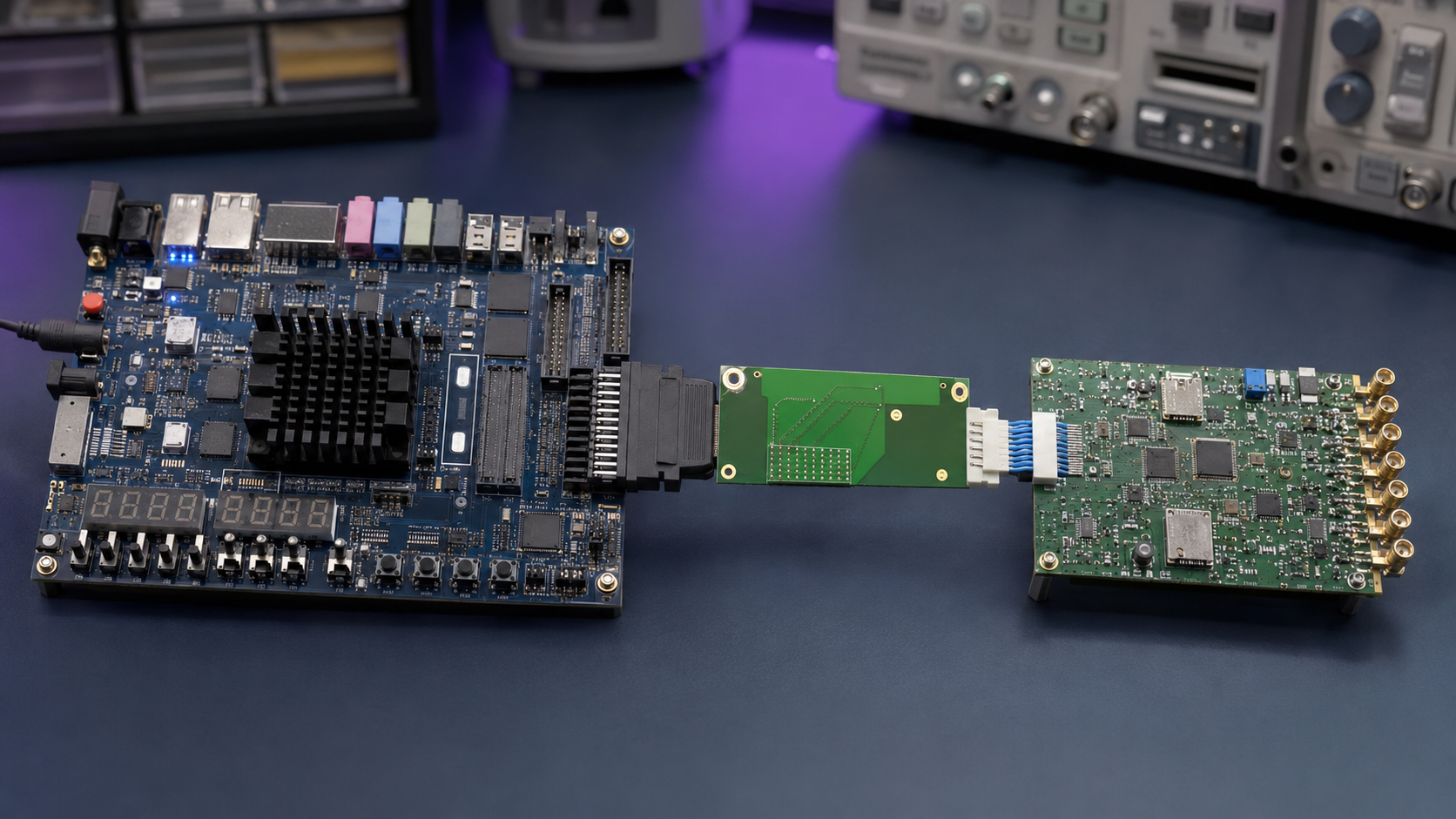
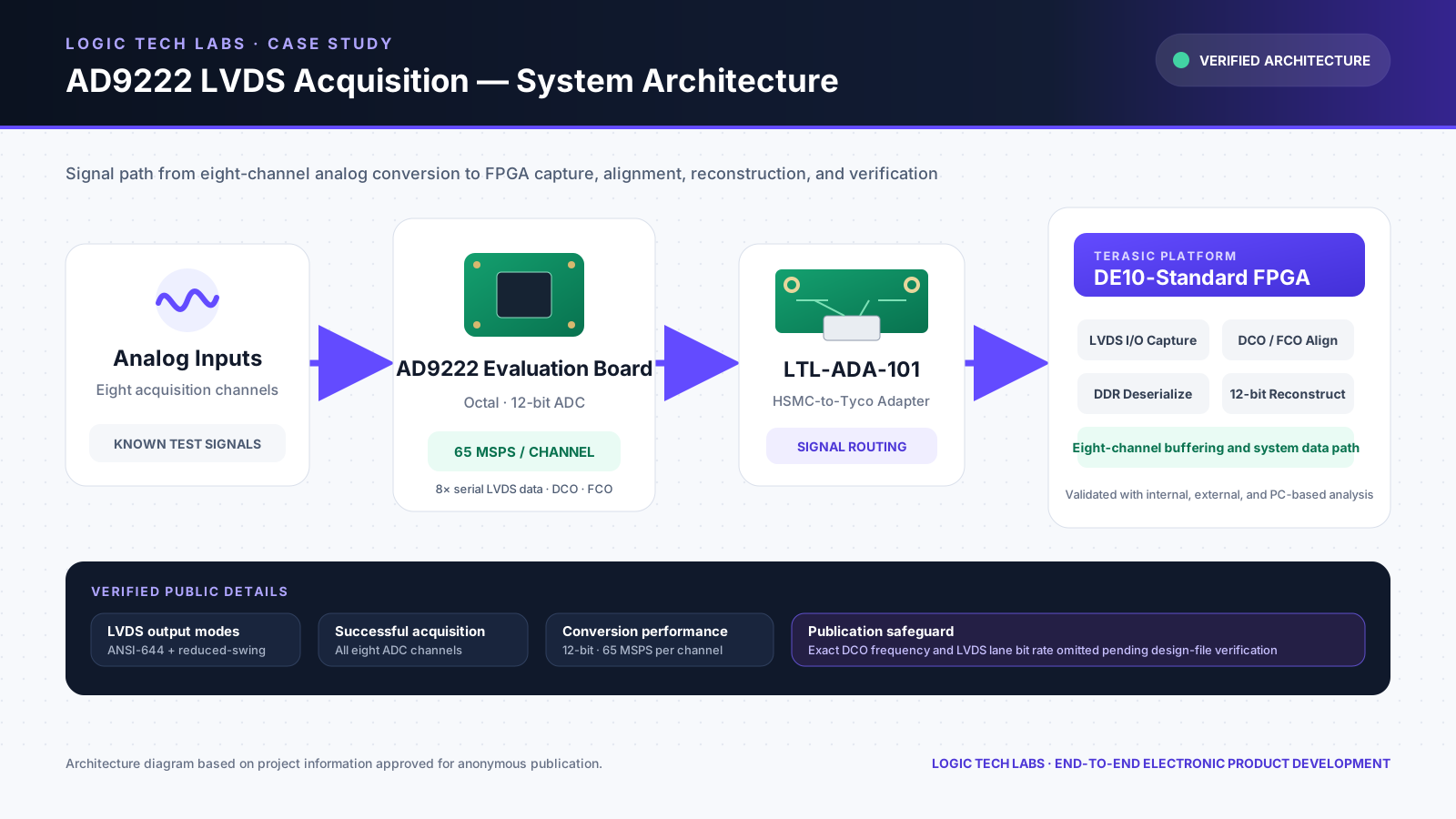
An end-to-end data-acquisition platform that receives all eight serial-LVDS outputs from an AD9222 evaluation board, reconstructs 12-bit samples in FPGA logic, and moves captured data through embedded Linux to a host computer over Ethernet.
- Engagement
- 3–6 month development program
- Platform
- Terasic DE10-Standard + AD9222
- Outcome
- Integrated and used operationally
Project objective
Turn eight high-speed LVDS streams into usable host data
The project covered the physical adapter, FPGA receiver, embedded-Linux integration, Ethernet transport, host software, and evidence-based validation as one coordinated system.
✓
Verified project factsResults and architecture statements are limited to approved project records.
A
Anonymized identityCustomer and identifying project details are withheld.
i
Illustrative visualsGenerated or simulated figures are explicitly identified in their captions.
Engineering challenge
Three tightly connected problems
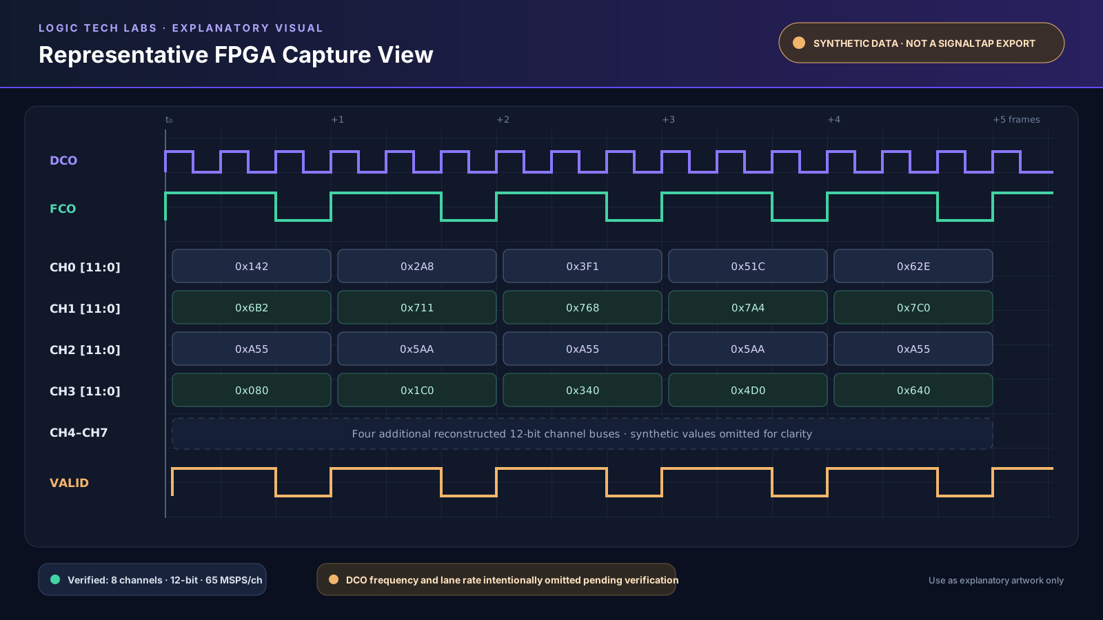
Implement dependable data-clock, frame-clock, bit, word, and channel alignment inside the FPGA.
Integrate the FPGA data path with the DE10-Standard HPS, embedded Linux, and host-side acquisition software.
End-to-end scope
One architecture across board, logic, Linux, and host software
Owning the interfaces between disciplines made it possible to debug the complete acquisition chain instead of treating each layer in isolation.
Requirements and architecture
Defined the acquisition, control, buffering, host-transfer, and verification architecture around the AD9222 evaluation platform.
LTL-ADA-101 adapter
Developed the HSMC-to-Tyco schematic and PCB, then coordinated fabrication and assembly for the physical ADC-to-FPGA interface.
FPGA RTL
Implemented the LVDS receiver, clock and frame alignment, channel reconstruction, buffering, control, and acquisition modes.
Embedded Linux
Built the HPS-side acquisition and control application for the DE10-Standard embedded-Linux environment.
Ethernet and host software
Implemented TCP and UDP transfer paths plus host tools for reception, storage, export, visualization, and analysis.
Verification and handover
Completed simulation, on-board debug, instrumented validation, documentation, and integration support for operational use.
Verified results
A complete acquisition path proven on target hardware
The delivered system supported both continuous and triggered/block capture and was integrated into the customer’s operational system.
- 8
- simultaneous ADC channels
- 12-bit
- reconstructed sample width
- 65 MSPS
- validated per channel
- TCP + UDP
- Ethernet transfer modes
Verified project outcome
Operational FPGA and embedded-Linux acquisition solution
Logic Tech Labs delivered a complete FPGA and embedded-Linux acquisition solution for the AD9222 evaluation platform. The operational system captured all eight 12-bit channels at 65 MSPS per channel, supported continuous and triggered acquisition, and transferred data through the DE10-Standard HPS using TCP/UDP over Ethernet.
Verified project result · Anonymous case studyVerification strategy
Correlating evidence across the full data path
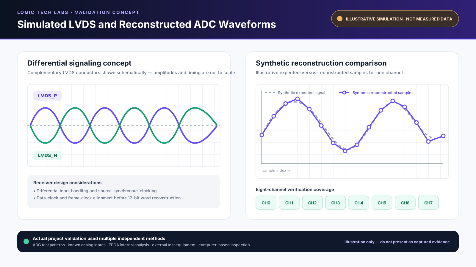
Simulation, converter test patterns, FPGA instrumentation, laboratory instruments, known analog inputs, and host-side inspection were used together.
- ✓AD9222 built-in test patterns
- ✓Known analog input signals
- ✓SignalTap internal FPGA analysis
- ✓Oscilloscope and external logic-analyzer checks
- ✓Host-side inspection of received data
Technology stack
Tools and platforms used across the system
The project combined RTL, embedded software, Ethernet applications, board-level engineering, and laboratory instrumentation.
AD9222Terasic DE10-StandardHSMCLTL-ADA-101Serial LVDSVHDLSystemVerilogCQuartus PrimeSignalTapModelSim / QuestaEmbedded LinuxTCP / UDP Ethernet
i
Technical disclosure: the validated sample rate is 65 MSPS per channel. Exact DCO frequency and serial-lane bit rate are not published here until they can be checked against the original design files.
Continue with the engineering details
Related technical guides
Engineering inquiry