
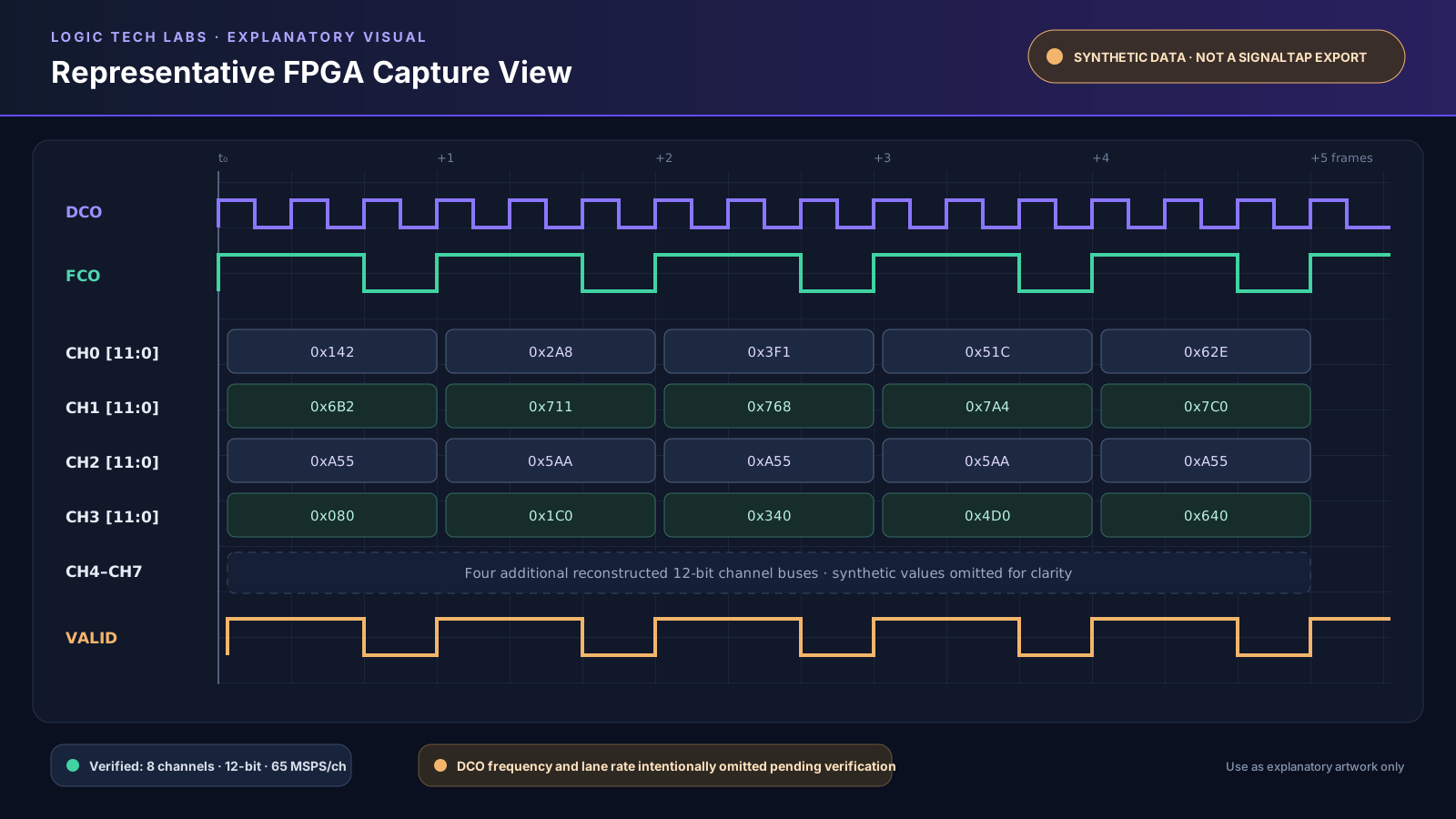
A multi-channel ADC receiver fails in more ways than a single serial link. Every lane must be captured with margin, all lanes must agree on the sample boundary, resets must produce deterministic state, and the complete channel group must cross into the processing domain without mixing samples from different conversion instants.
A good architecture makes these risks observable. It exposes alignment status and error evidence, preserves clean clock-domain boundaries, and supports test modes that isolate the physical link from the analog signal chain.
Key engineering takeaways
- ✓Keep serial capture, word assembly, channel-group alignment, CDC, and transport as separate reviewed layers.
- ✓Use the forwarded data clock for capture and move only complete framed samples into the system domain.
- ✓Make alignment measurable with lock state, pattern comparators, counters, and triggerable capture points.
- ✓Design reset and re-alignment behavior before optimizing throughput.
- ✓Validate lane margin and system behavior, not only a short correct-looking waveform.
1. Treat the link as a source-synchronous interface
In a source-synchronous link, the transmitter forwards a clock alongside the data. The receiver should capture the incoming data relative to that forwarded clock, not relative to an unrelated system oscillator. This local relationship is the foundation of the input timing model.
The capture clock and the later processing clock may have different frequencies, phases, reset behavior, or stability assumptions. That makes the boundary between them a real clock-domain crossing, even if both ultimately originate from the same board.
2. Build the receiver as six explicit layers
The layers below are useful as both an RTL partition and a verification plan. Each layer has a specific contract and a small set of failure indicators.
| Layer | Responsibility | Useful evidence |
|---|---|---|
| Physical input | Differential buffering, pin mapping, electrical standard | Pin audit, polarity check, bank configuration |
| Bit capture | DDR or serial sampling in the forwarded-clock domain | Timing report, test-pattern bit stream |
| Word assembly | Reconstruct the configured sample width and bit order | Expected repeating words, word counter |
| Frame alignment | Establish and maintain the sample boundary | Lock state, slip count, alignment error |
| Channel grouping | Present one coherent sample vector across all lanes | Channel-valid pulse, group sequence number |
| CDC and buffering | Move complete vectors into the processing domain | FIFO levels, overflow/underflow counters |
3. Use FPGA input resources deliberately
Modern FPGAs provide differential input buffers, input DDR registers, delay elements, deserializers, and regional or global clock networks. Which resources are appropriate depends on the FPGA family, lane rate, pin placement, clock topology, and required margin.
Place the first sampling stage close to the I/O boundary. Avoid adding general fabric logic in front of the capture registers. If adjustable delay is used, define how it is calibrated, stored, re-applied after reset, and checked across voltage and temperature.
- Review clock-capable pin placement before freezing the PCB pinout.
- Keep the data and forwarded clock in compatible I/O regions when the FPGA architecture requires it.
- Constrain input timing with datasheet and board-delay assumptions.
- Record any lane-specific inversion, delay, or bit-slip state as configuration data.
4. Make alignment a state machine, not a hope
A receiver should define how it enters alignment, how it confirms alignment, what causes it to declare loss of lock, and how it recovers. A frame clock or known training pattern can establish the word boundary; a continuous checker can then confirm that the expected relationship remains intact.
For multiple channels, alignment must be evaluated at group level. A valid sample vector should represent the same conversion instant on every channel. If independent per-lane buffering is used, include a deterministic method to equalize and monitor lane latency.
5. Cross clock domains only after the sample is complete
Crossing individual bits or partially assembled words creates unnecessary coherence risk. Reconstruct and validate the complete channel group in the acquisition domain, then transfer it through a reviewed CDC structure.
An asynchronous FIFO is a common choice when the acquisition and processing clocks are independent or burst behavior is expected. Size the FIFO from worst-case production and consumption rates, allowed backpressure, trigger behavior, and host-service latency. Add overflow and underflow counters and make them visible to software.
6. Verify the receiver in layers
Simulation should exercise both correct and incorrect behavior: polarity swaps, bit-order errors, frame displacement, reset during traffic, missing clocks, stalled consumers, and FIFO overflow. Target-hardware validation should then correlate converter test patterns, FPGA internal instrumentation, laboratory measurements, and host data.
A short successful capture demonstrates functionality at one moment. Reliability needs repeated startup, long-duration acquisition, reset recovery, and operation across the intended clock and configuration range.
- 01
Unit simulation
Verify capture-to-word logic with controlled serial patterns and edge relationships.
- 02
CDC checks
Apply structural CDC analysis and simulate asynchronous clock ratios and reset ordering.
- 03
ADC test mode
Use a repeatable converter pattern to separate digital alignment from analog behavior.
- 04
Known analog stimulus
Confirm sample order, amplitude, channel mapping, and expected waveform behavior.
- 05
Stress and recovery
Exercise long runs, repeated resets, triggers, host stalls, and configuration changes.
Primary references
Sources and further reading
- Analog Devices — AD9222 data sheet ↗
- Analog Devices — HSC-ADC-FPGA deserialization board data sheet ↗
- Texas Instruments — LVDS Application and Data Handbook ↗
External documents remain the authority for component ratings, standard requirements, and device-specific implementation details.