
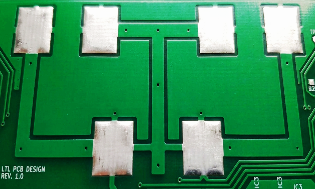
A high-speed acquisition system is a chain of coupled design decisions. Converter clock quality affects sampled data; board geometry affects the digital eye; FPGA pin placement affects routability and clock access; reset and buffering affect whether a correct sample reaches the host.
Reliability improves when the PCB, FPGA, firmware, and validation plan are reviewed together. Optimizing one layer while leaving an incompatible assumption in another produces systems that work intermittently or only on one prototype.
Key engineering takeaways
- ✓Define the acquisition data path and timing budget before schematic and FPGA pin assignment diverge.
- ✓Use the PCB fabricator's controlled stack-up to calculate routing geometry.
- ✓Review connector transitions, return paths, termination, and FPGA pin classes as one interconnect.
- ✓Separate clean acquisition power and clocking from noisy digital activity with intentional placement and distribution.
- ✓Design measurement access and internal observability before the first prototype arrives.
1. Begin with a system budget
Capture sample rate, channel count, resolution, serialization, clock relationships, sustained and burst throughput, trigger latency, buffering, and host-transfer assumptions. This exposes whether the proposed connector, FPGA resources, memory path, and software service rate are compatible.
Include margin and failure behavior. Define what happens when a host stalls, a trigger arrives during a transfer, alignment is lost, or the FIFO reaches a threshold. A throughput calculation without backpressure and recovery behavior is incomplete.
2. Treat the clock as part of the analog signal chain
Sampling-clock jitter can degrade signal-to-noise performance, especially as input frequency increases. Clock-source selection, power filtering, fan-out, routing, termination, and proximity to noisy digital regions should be reviewed against the converter's requirements.
For the digital interface, define which clock captures each signal and how that clock enters the FPGA. Keep the sample clock, forwarded data clock, frame clock, processing clock, and host clock distinct in the architecture even when they are related.
3. Plan power distribution for both noise and transients
Converter analog rails, digital output rails, FPGA I/O banks, FPGA core supplies, clock devices, and high-current digital loads have different noise and transient behavior. The design needs appropriate regulators, decoupling, return paths, sequencing, and measurement points.
Use current estimates that include startup and dynamic conditions. Review regulator stability with the selected capacitors and layout. Provide a safe method to measure rail voltage, ripple, and startup ordering during bring-up.
4. Control the interconnect from package to package
Differential impedance, intra-pair symmetry, reference-plane continuity, via transitions, stubs, connectors, and termination determine how much of the transmitter eye reaches the receiver. The path must be reviewed end to end, including any adapter or cable between boards.
Texas Instruments' LVDS layout guidance recommends 100-ohm differential traces, close coupling, equal length within a pair, short direct routing, minimized stubs, and receiver-side termination placement. These are design principles; the actual dimensions must come from the chosen stack-up and field-solver or fabricator guidance.
- Avoid crossing reference-plane splits with high-speed return currents.
- Maintain pair geometry through bends and mirrored discontinuities.
- Limit via use and review via return paths where transitions are unavoidable.
- Separate unrelated high-edge-rate signals enough to control crosstalk.
- Review connector pin assignments for adjacent grounds and pair continuity.
5. Perform FPGA pin and timing planning before layout
Pin selection affects I/O bank voltage, differential capability, clock routing, regional resources, package skew, and PCB escape. A schematic pin table should be checked against the FPGA device database and a small compile or pin-planning project before the layout is frozen.
Create source-synchronous timing constraints early and verify that the planned input resources can meet them. If the design depends on adjustable delay or particular SERDES placement, prove resource availability before committing the PCB.
6. Design for bring-up and fault isolation
Add access for rail measurement, resets, clocks, configuration, and selected digital signals. In the FPGA, include version registers, build identifiers, alignment status, counters, FIFO levels, test-pattern checking, and internal capture triggers.
The objective is not to expose every node. It is to create enough independent evidence to decide whether a failure originates in power, clocking, physical I/O, framing, CDC, buffering, firmware, or host transport.
Primary references
Sources and further reading
- Texas Instruments — High-Speed Layout Guidelines for LVDS SerDes Designs ↗
- Texas Instruments — LVDS Application and Data Handbook ↗
- Analog Devices — AD9222 data sheet ↗
External documents remain the authority for component ratings, standard requirements, and device-specific implementation details.